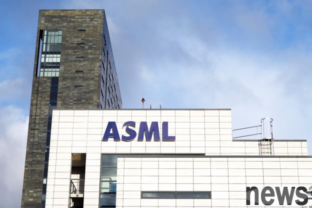
Xu Kuancheng, customer marketing director of ASML Taiwan and Southeast Asia at semiconductor lithography equipment factory, said on the 19th that semiconductor process technology continues to shrink, and High NA EUV equipment will help customers save time and costs. Currently, customers include Intel, IBM and Samsung, and more than 350,000 wafers have been exposed using High NA EUV.
ASML held a media exchange meeting on the 19th. Xu Kuancheng said that today’s society is transforming from the ubiquity of chips to the ubiquity of artificial intelligence (AI). AI will drive the growth of demand for advanced and mature semiconductor processes, and global semiconductor sales are expected to exceed the US$1 trillion mark in 2030.
Xu Kuancheng said that although Moore's Law has challenges, it will continue to develop in the direction of Moore's Law in the next 10 to 15 years, and semiconductor process technology will continue to shrink. Moore's Law means that as process technology improves, the density of transistors that can be accommodated on a chip will double approximately every 18 to 24 months.
Xu Kuancheng said that in the past, when immersion lithography was promoted to extreme ultraviolet (EUV) lithography equipment, there was noise in the industry. Currently, High NA EUV is facing the same situation.
ASML’s High NA EUV customers include Intel, IBM and Samsung, and a total of more than 350,000 wafers have been exposed using High NA EUV equipment. Xu Kuancheng said that High NA EUV equipment helps customers save time and costs due to its higher imaging quality and simplified process advantages.
Xu Kuancheng pointed out that ASML continues to improve its deep ultraviolet (DUV) lithography equipment to help customers meet a large number of DUV exposure needs at a lower cost. In addition, XT:260 was launched to support advanced packaging applications.